


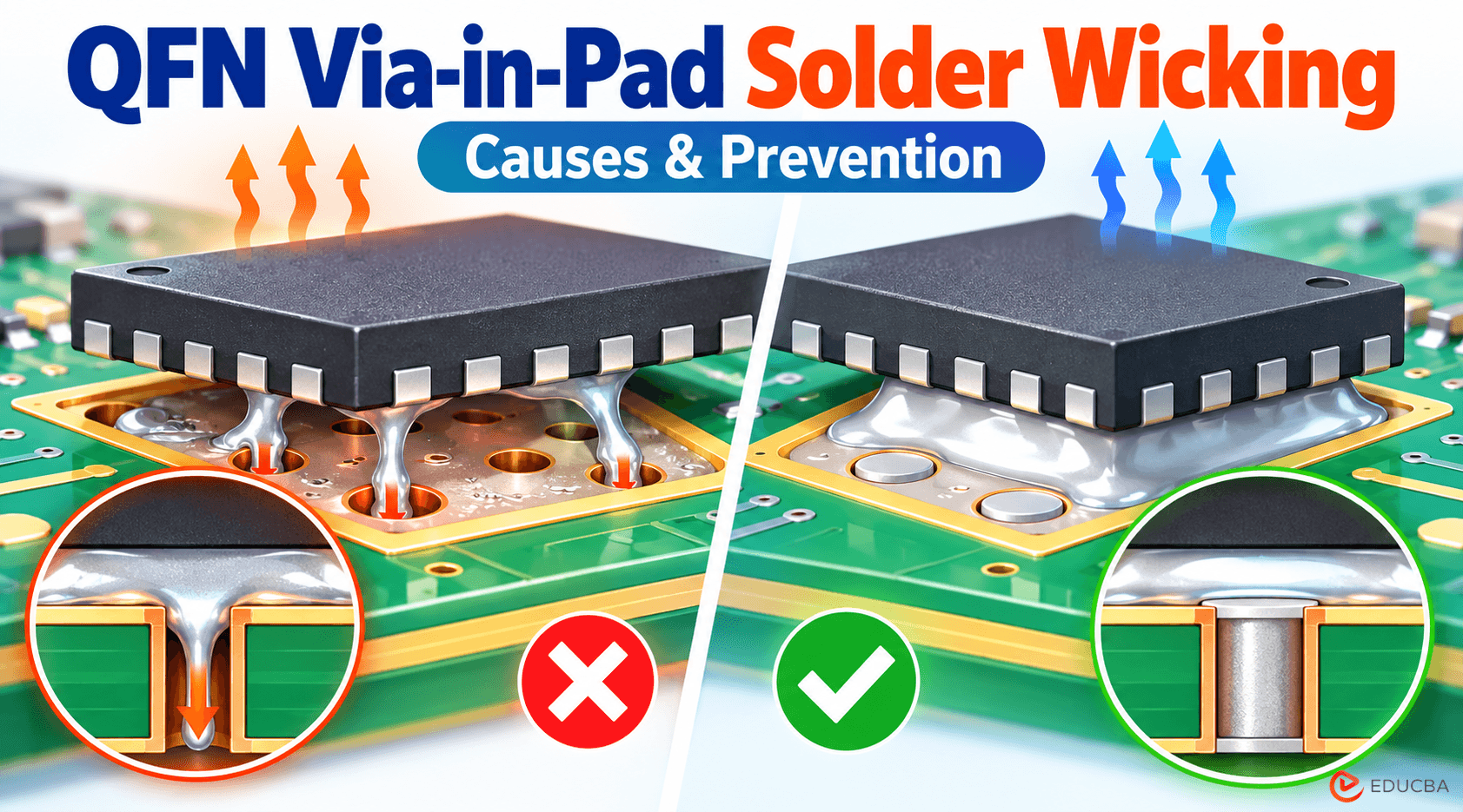
QFN packages use PCB area efficiently, provide short electrical paths, and often offer good thermal performance through an exposed center pad. However, that same exposed pad creates a manufacturing problem when thermal vias are placed directly inside the land pattern.
If those vias are left open, molten solder can migrate into the holes during solder reflow. This phenomenon, known as QFN via-in-pad solder wicking, can cause solder drainage and affect final assembly quality. In mild cases, the assembly may still pass electrical testing. In more severe cases, the QFN can end up with insufficient solder beneath the exposed pad, excessive voiding, package tilt, or inconsistent thermal performance.
The issue is not simply “too many vias.” It is the interaction between via construction, stencil design, solder paste volume, surface finish, and the reflow process.
What Causes QFN Via-in-Pad Solder Wicking?
During reflow, solder paste deposited on the exposed pad passes through several stages. Flux activates, solder particles coalesce, and the alloy becomes fully molten.
At this point, any plated through-hole inside the pad can become a path for liquid solder.
A conventional via consists of a plated copper barrel extending through the PCB. If the via is open at the surface, molten solder can wet the copper plating and move down the barrel through wetting forces, gravity, pressure differences, and capillary behavior.
Some solder may remain underneath the QFN, but some can migrate toward the opposite side of the board.
- Solder loss: too much solder leaves the component interface.
- Void formation: gases or flux residues become trapped within the solder joint.
The two can occur together, but you should not treat them as the same defect. A board can have substantial voiding without serious solder drainage, and it can also lose solder through vias without producing one large visible void.
Why the QFN Thermal Pad Is Particularly Sensitive?
For many QFNs, the center exposed pad performs both mechanical and thermal functions. Depending on the component, it may also be electrically connected to ground.
Unlike perimeter leads, the exposed pad covers a relatively large copper area. Designers often add multiple vias to transfer heat into internal or bottom copper planes.
That improves thermal conduction, but it also creates multiple solder escape paths. Open vias inside the thermal pad can cause QFN via-in-pad solder wicking, which reduces the solder available to form a reliable joint.
When engineers place ten or twenty open vias inside the thermal pad, even a small amount of solder entering each via can significantly reduce the total solder volume beneath the package.
- Reduced thermal contact area
- Increased thermal resistance
- Uneven package stand-off
- Solder protruding on the PCB underside
- Excessive center-pad voiding
- Variation from board to board
- Increased sensitivity to rework and repeated thermal cycling.
A prototype may still operate normally, which can make the problem easy to underestimate. The defect may only become obvious after production volume increases.
Open, Tented, Filled, and Capped Vias Are Not Equivalent
Open Vias
Open vias provide the most direct path for solder migration. If the via opening is exposed inside the QFN thermal pad, solder can enter the barrel during reflow.
For low-cost assemblies, open thermal vias may still be usable, but you must carefully control stencil design and via geometry.
Tented Vias
A tented via is covered with solder mask on one or both sides.
Tenting from the opposite side can reduce solder emerging on the bottom of the PCB, but it does not necessarily eliminate solder movement into the via barrel. Entrapped air and flux can also introduce their own process concerns.
For that reason, simply specifying “tented vias” should not automatically be considered equivalent to a filled via-in-pad structure.
Filled and Capped Vias
For demanding QFN, BGA, and fine-pitch designs, a filled and capped via-in-pad is often the more controlled solution.
The via cavity is filled, typically with resin, and the surface is planarized and copper plated. This creates a much flatter, more continuous pad surface.
In fabrication terminology, this is commonly associated with filled-and-capped via structures described under IPC-4761 via protection classifications.
The main manufacturing advantage is straightforward: no open barrel lies immediately beneath the solder paste deposit.
However, filled and capped vias increase PCB fabrication cost and require tighter process control. They should therefore be specified where the reliability or assembly benefit justifies them.
How Stencil Design Affects QFN Via-in-Pad Solder Wicking?
Closing the vias does not automatically guarantee a good QFN joint.
Depositing one large block of solder paste across the entire exposed pad often creates too much solder and can trap large volumes of flux.
A windowpane-style pattern can help control total paste volume and provide paths for gases to escape during reflow.
- QFN dimensions
- Exposed-pad area
- Stencil thickness
- Solder paste type
- Via arrangement
- Target thermal performance
- Package supplier recommendations.
A common mistake is optimizing the PCB copper pattern while treating the stencil as an afterthought. For QFN assembly, review PCB land design and stencil design together.
Via Diameter and Via Density Matter
Larger holes can carry more solder, but reducing via diameter is not a complete solution.
A thermal pad containing many small open vias may still lose a meaningful amount of solder because the total open area remains large.
Designers should evaluate total via opening area, not simply individual drill size.
Designers must also consider the thermal objective. Reducing the number of vias too aggressively can improve soldering while degrading heat transfer.
- Thermal conductivity
- PCB fabrication capability
- Solder paste retention
- Assembly yield
- Reliability requirements.
There is no universal via count that works for every QFN.
How QFN Via-in-Pad Solder Wicking Appears in Production?
Visual inspection has limited value because the critical solder joint is underneath the component.
X-ray inspection is much more useful.
- Irregular solder coverage under the thermal pad
- Localized areas of low solder volume
- Large or clustered voids
- Asymmetrical solder distribution
- Evidence of solder entering thermal vias.
However, interpret X-ray results carefully. A dark or light region does not by itself prove that solder wicking is the root cause.
The assembly team should compare X-ray results with the PCB stack-up, via construction, stencil file, paste volume, reflow profile, and bottom-side inspection.
Cross-sectioning may be required during failure analysis when the mechanism cannot be confirmed non-destructively.
Reflow Profile Can Influence the Result
Via geometry is usually the dominant design factor, but reflow conditions can amplify the problem.
- Soak time
- Peak temperature
- Time above liquidus
- Heating rate
- Flux chemistry
- PCB thermal mass.
Longer periods with the solder fully molten give solder more opportunity to redistribute.
Changing the reflow profile should therefore not substitute for correcting a fundamentally poor via-in-pad design. Process optimization can improve margins, but it cannot completely compensate for an uncontrolled solder escape path.
How to Prevent QFN Via-in-Pad Solder Wicking?
Before releasing a QFN board for production, review the exposed pad as one manufacturing system rather than as separate PCB and SMT features.
- Are any vias open directly inside the solderable pad?
- What is the total open via area?
- Are the vias tented, plugged, filled, or filled and capped?
- Does the component manufacturer specify a recommended thermal-via pattern?
- Is the stencil aperture segmented?
- Is the total paste coverage appropriate for the package?
- Will solder be able to reach the PCB underside?
- Is X-ray inspection available for first-article verification?
For high-reliability or high-volume designs, resolve these questions before tooling rather than after the first assembly run.
Engineers who need to compare filling methods, materials, and IPC-4761 classifications can refer to this guide to PCB via filling before defining the fabrication notes.
A capable PCB assembly service can also review the Gerber data, stencil design, via construction, and package requirements together before production begins.
The Real Issue Is Process Interaction
Via-in-pad is not inherently a bad design practice. In many QFN applications, it is essential for thermal performance.
The problem begins when thermal vias are treated only as PCB features rather than as part of the solder joint.
An open via changes how solder behaves during reflow. A filled and capped via changes the pad surface. Stencil geometry controls the available solder volume. Reflow conditions determine how long that solder can move.
Reliable QFN assembly therefore depends less on one isolated design rule and more on controlling all of these variables as a single system.
For engineers working with exposed-pad packages, the key point is this: thermal performance and solderability must be designed together.
Recommended Articles
We hope this guide helps you understand QFN via-in-pad solder wicking, including its causes, prevention methods, via designs, stencil requirements, and reflow considerations. Explore our recommended articles for more insights on PCB design, soldering techniques, surface-mount technology, and PCB assembly.